
onsemi FDD4141: Key Specifications and Application Circuit Design Considerations
The onsemi FDD4141 is a robust Field Effect Transistor (FET) engineered for high-performance power management applications. As a member of the renowned PowerTrench® MOSFET family, it is specifically designed to deliver high efficiency and reliability in demanding switch-mode power systems. Understanding its key specifications and the nuances of its application circuit design is crucial for engineers to fully leverage its capabilities.
Key Specifications
The FDD4141 is an N-channel MOSFET characterized by several critical parameters that define its operational boundaries and performance.
Drain-Source Voltage (VDSS): 100 V. This rating specifies the maximum voltage the device can block between drain and source, making it well-suited for applications like 48V input power systems, DC-DC converters, and motor control circuits.
Continuous Drain Current (ID): 9.7 A at a case temperature (TC) of 25°C. This is the maximum continuous current the FET can handle. It is vital to consider derating this value based on the actual operating temperature and thermal management.
On-Resistance (RDS(on)): A maximum of 62 mΩ at VGS = 10 V, ID = 4.85 A. This exceptionally low value is a hallmark of the PowerTrench process, leading to reduced conduction losses and higher overall efficiency. Lower RDS(on) directly translates to less heat generation during the on-state.
Gate Threshold Voltage (VGS(th)): Ranging from 2.0 V to 4.0 V. This defines the minimum gate-to-source voltage required to turn the device on. This range is standard for a logic-level FET, but ensuring a sufficient gate drive voltage above the maximum threshold is key for full enhancement.
Total Gate Charge (Qg): 24 nC (typical). This parameter is crucial for determining switching performance. A lower gate charge allows for faster switching speeds and reduces drive power requirements, which minimizes switching losses.
Application Circuit Design Considerations
Successfully integrating the FDD4141 into a design requires careful attention to several circuit aspects.
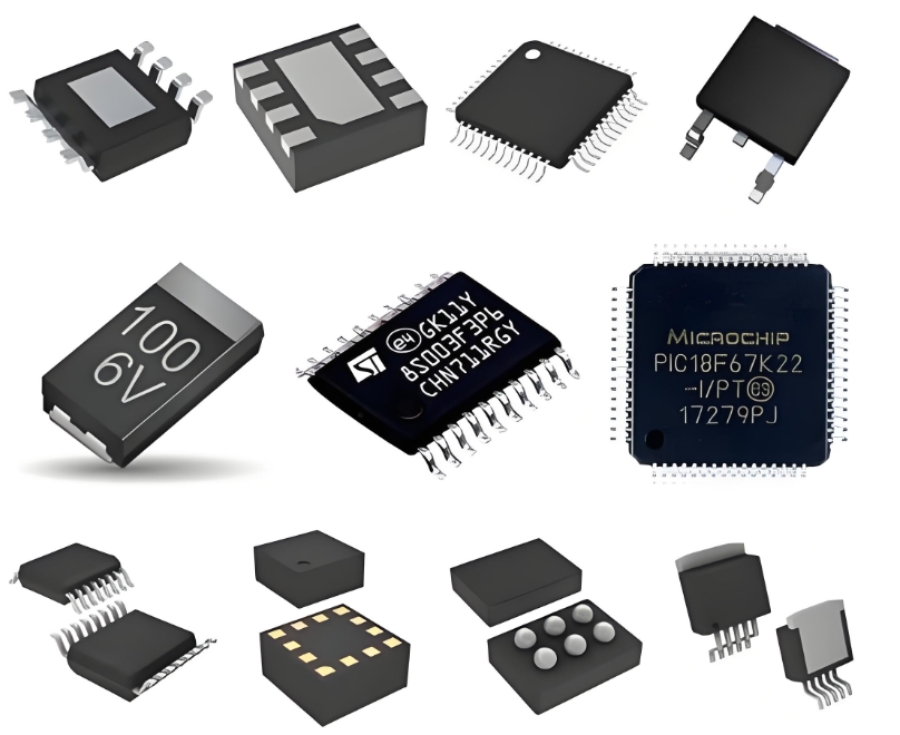
1. Gate Driving: To achieve fast switching and avoid operating in the linear region (which causes excessive heat), a dedicated gate driver IC is highly recommended. The driver must be capable of sourcing and sinking sufficient peak current to rapidly charge and discharge the MOSFET's gate capacitance. The gate drive voltage should be comfortably above the VGS(th) max, typically between 10V and 12V, to ensure low RDS(on).
2. Protection Mechanisms:
Voltage Spikes: Switching inductive loads can cause dangerous voltage spikes across the drain and source. A snubber circuit or a Transient Voltage Suppression (TVS) diode may be necessary to clamp these spikes and prevent VDSS from being exceeded.
Overcurrent Protection: Implementing current sensing (e.g., with a shunt resistor) and a protection circuit is essential to safeguard the MOSFET and the overall system from fault conditions that could lead to catastrophic failure.
3. Thermal Management: Despite its low RDS(on), power dissipation (I²R losses) can still generate significant heat, especially at high currents. Proper heatsinking is non-negotiable. The design must ensure that the junction temperature (TJ) remains safely below the absolute maximum rating of 150°C. Calculating power dissipation and thermal impedance (RθJA) is a critical step in the PCB layout process.
4. PCB Layout: A poor layout can introduce parasitic inductance and capacitance, leading to oscillations, voltage overshoot, and EMI issues. Key practices include:
Minimizing loop areas for both the power switching path and the gate drive circuit.
Using short and wide traces for high-current paths.
Placing the gate driver close to the MOSFET gate pin.
Utilizing multiple vias to connect to ground and power planes for lower impedance and better thermal dissipation.
ICGOODFIND: The onsemi FDD4141 stands out as an excellent choice for power designers seeking a balance of high voltage capability, low on-resistance, and fast switching performance. Its effectiveness is maximized not just by its datasheet specifications, but through meticulous attention to gate driving, protection, thermal design, and PCB layout. By adhering to these design considerations, engineers can build efficient, reliable, and robust power electronic systems.
Keywords: Power MOSFET, On-Resistance, Gate Driver, Thermal Management, Switching Performance

